Solid State Electronics
General level Solid State covering electronic properties, i.e. Band Theory, Types of Metals, Mott-Hubbard Insulators, Trends in Metals, Superconductors and special examples, then Defects and Ionic Conductivity. Little bit on Experimental Methods at the end.
Solid State - Electronics
A) Bonding and Electronic Properties of Solids
What are bands?
When looking at the bonding properties in solids, it is possible to continue to use the LCAO approach as for molecules, but think of the solid as essentially a huge molecule. Thus, many molecular orbitals form and are very closely space in energy. Orbitals extend throughout the solid, and are referred to as crystal orbitals. It is reasonable to neglect the spacing between so many orbitals, and this gives rise to continuous bands of energy levels.
Derivations – LCAO (tight binding) approach:
Consider an infinite periodic solid.
ψ(x + Na) = ψ(x) [ Periodic Boundary Condition, large N ]
ψ*(x + a) ψ(x + a) = ψ*(x)ψ(x) [ Periodic, so electron density is the same ]
From this, μ(x + a) = μ(x) & μμ* = 1
Combining the two above,
ψ(x + Na) = μNψ(x)
Therefore μN = 1, → μ = e2piπ/N
This is usually written with: k = 2πp/Na , where p is an integer and k is a quantum number.
Hence,
ψ(x + a) = eikaψ(x) and eika is the phase difference.
Generally,
ψ(x) = eikx u(x) [ u(x) is any periodic function ]
This is the Bloch Criterion. In Band Theory, wavefunctions must satisfy this.
The LCAO approach gives k as a wavevector, whereas the free electron approach treats it as a momentum vector.
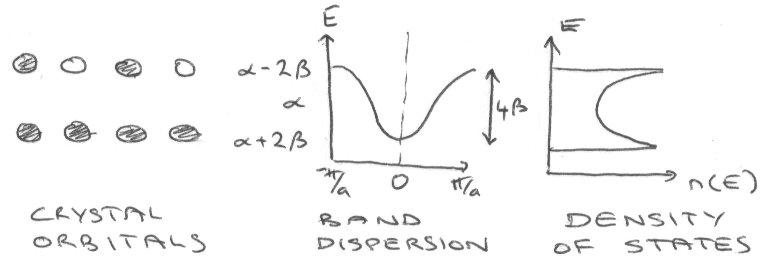
Using the LCAO approach for a 1 dimensional chain:
ψ(x) = Σ cnφn(x) & cn = eikna (Bloch)
k = 2πp/Na where there are N atoms in the chain, and the 1st Brillouin zone is taken as:
–π/a ≤ k ≤ π/a with N unique values of k.
N being arbitrarily large means that k is a continuous variable, and so a continuous band is formed.
Important Consequences –
Wavefunctions for crystal orbitals are characterised by k. It defines the phase relationship between adjacent s orbitals in the chain.
k = 0 → phase factor = 1, so adjacent orbitals are in phase and this gives the maximally bonding configuration.
k = π/a → phase factor = -1, so adjacent orbitals are out of phase to give the maximally antibonding configuration.
k = π/na → n lattice spacing along the chain to find an orbital out of phase.

Also, k is related to wavelength by λ = 2π/k. This is where the limits of the 1st Brillouin Zone come from – it is the volume of reciprocal (k) space for the limits 2a < λ < ∞.
The Dispersion relationship gives the energies of different states relation to the wavevector:
EK = α + 2β cos (ka),
Where α = energy of the atomic s orbital, and β = Huckel parameter (a measure of the strength of the interaction between orbitals on adjacent atoms – overlap).
β < 0 and maximally bonding states with k = 0 gives E = α + β.
Maximally antibonding states gives E = α − 2β.
Hence β is a measure of the energy width of the band. Overlap strongly → broad in energy.
Density of States, n(E).
n(E) dE = number of allowed energy levels per unit volume of the solid in the energy range E → E+dE.
n(E) = 0 in the forbidden band gaps.
This describes the allowed crystal orbitals evenly distributed in k-space.
Using the definition of k and the Dispersion Relationship:
n(E) = dn/dE = (dn/dk) / (dE/dk) = -1/2π(1/2βa sin ka).
i.e. n(E) is a maximum at the edges of the band where the dispersion is flat.
Comparison with Nearly-free Electron Model -
The Free Electron Model treats electrons as confined to a 3D box of side length L. Solutions of the Schrodinger Equation in 3 dimensions take the form:
ψk(r) = eikr
r = a position vector in polar coordinates, and k2 = kx2 + ky2 + kz2, and k is a quantum number.
The solutions give rise to free electron waves. λ = 2π/k so p = h/λ gives p = hk (i.e. k is a momentum vector).
Removal of the finite size of the box by applying the periodic boundary condition restricts the quantum numbers such that:
kx = 0, ±2π/λ, ±4π/λ, etc.
This means that energies are quantised, and also means that k is not restricted, and the dispersion has no gaps. This clearly cannot be true, as all materials would be metals! This is compensated for by saying that electrons do experience a Periodic potential of atomic cores. Electron wavelengths which coincide with the periodicity of the lattice are diffracted by it, which gives the band gaps at ±nπ/a.
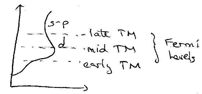
The nearly-free electron model works well for broad band systems such as the alkali metals (see below for Mg), while the LCAO approach works better for narrow band systems such as Transition Metal Oxides.
It can also be used for predicting specific heats of simple metals. This is particularly relevant for metals since bandwidths are huge compared to thermal energies (0.025eV at rtp). Only a few electrons are close to the Fermi Energy can be thermally excited at room temperature and thereby contribute to specific heat. Hence contribution from conduction electrons is much less than predicted by equipartition of Energies.
Populating the Bands –
Electrons fill the available levels according to the Pauli Exclusion Principle. Energy of the highest filled level is the Fermi Level, with Fermi Energy EF.
This represents the chemical potential of the electrons in a solid.
Relating Properties
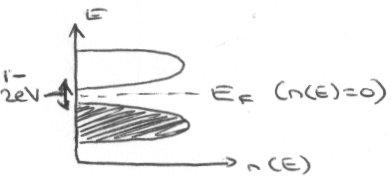
Consider Li and Be (both not well explained by the Free Electron Model). The 2s band is half filled for Li, which suggests metallic (which it is). However for Be the 2s is full, if not for overlap of the 2s and 2p bands. No overlap would imply non-metallic and non-cohesive (bonding and antibonding filled). PES / X-ray shows that there is a minimum density of states at the Fermi Level, which indicates poor overlap, but still some (non-zero).
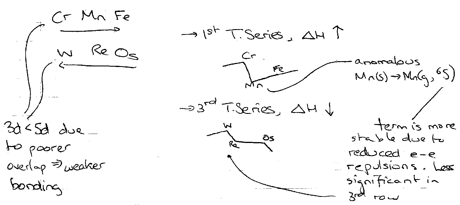
Transition Elements show good 4s and 3d overlap (4s is very diffuse). Cohesive Energy varies with extent of band filling, and expect a maximum when half-full. This is true for e.g. W. The dip at Mn is due to something else:
Mn(s) → Mn(g, 6S)
Ground 6S term is more stable than spin or orbital randomised average configurations, due to reduced electron-electron repulsions. This is less significant in the 2nd/3rd row hence W is high melting point. This all gives rise to the trends in melting point seen (see Transition Metal Chemistry Notes). Electron repulsion has much wider implications to properties (see later).
Cohesion Energy
This varies with the extent of band filling. Expect a maximum when ½ full (e.g. tungsten). The trends noted are:
Considering the Band Structure –


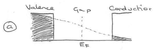
Covalent Solids
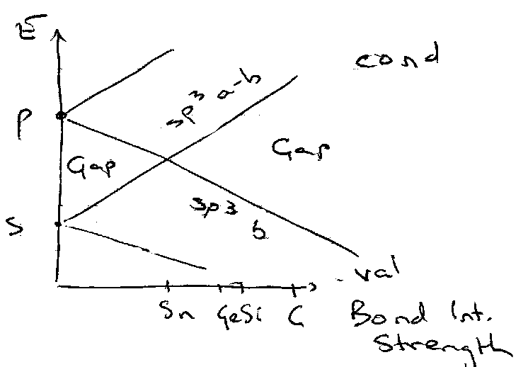


Sn/Pb → divalent chemistry as well (no s electron involvement). These appear to the left of the crossover point.
Group IV is surprising, as s2p2 is partially filled, but there is a band gap. Reason here is related to the structure – for example diamond (tetrahedral). Interatomic energy > intrinsic s-p separation, so treat as sp3 hybridised bonding / antibonding levels as basis of constructing bands. Thus the band gap approximately equals the bonding / antibonding energy level gap, and correlates to melting points.
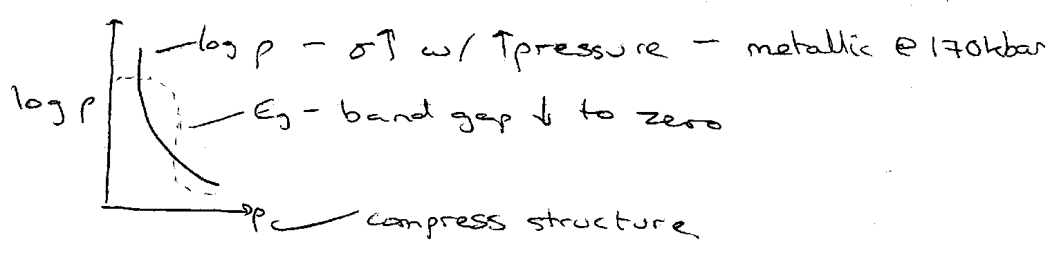
Molecular Solids have bands which form from the MOs instead of the AOs. For example, solid I2 has filled σg2, πu4, πg4 and empty σu. Increasing the pressure causes broadening of the bands generated from this, and can be sufficient for overlap of πg and σu bands, which leads to metallic properties.
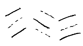
Layers of I2 molecules (lattice):
Example of polarisation catastrophe theory – predicts any solid tends to metallic properties at sufficiently high density.
Electrical conductivity is an obvious property of metallic solids. Each crystal orbital corresponding to motion of an electron in one direction will have another of the same energy corresponding to the reverse motion.
R = ρl/A = l/σA, where ρ is the resistivity (Ωm) and σ is the conductivity (Ω-1m-1).
Also, σ = A e-E/kT
Classes of Solid
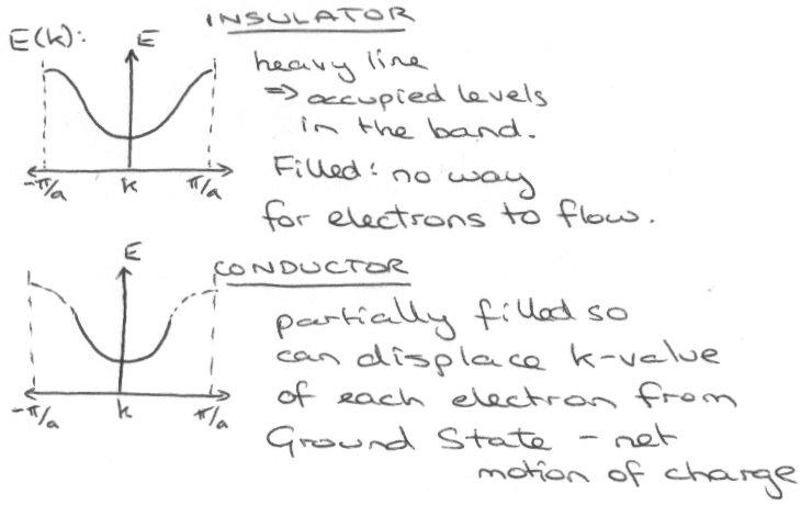
Insulator –
In a filled band, net motion of electrons cancels out, so no conductivity. Thus, an insulator gives bands as:

This is typified by a solid such as MgO:
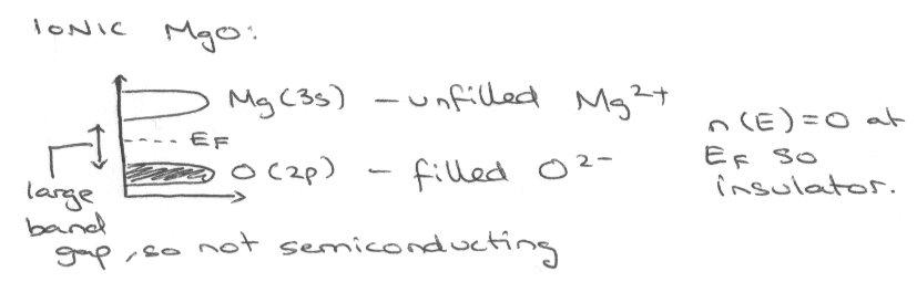
Oxides typically are strongly governed by Madelung Potentials, due to unstable free O2- ions.
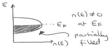
Metal –
But partially filled bands with no energy gap above the top occupied level means that electrons near the top-filled level can move into unfilled orbitals under the influence of an electric field – this gives motion of charge (conducts).
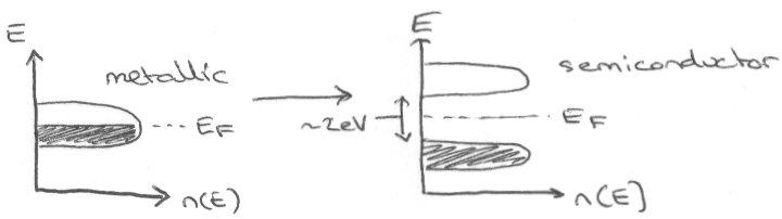
An unusual example is looking at the alkali metals. For example, Mg is metallic, but we would expect its band structure to appear as:
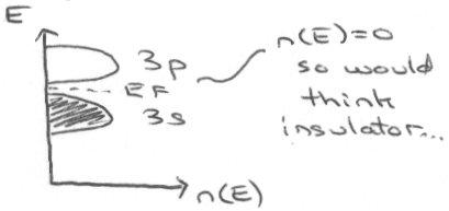
In fact, it conducts because of overlap of the 3s and 3p orbitals, so the above picture is not valid. There is an extended conduction band that develops because the 3s is very diffuse, and so its electrons can spill over into unfilled orbitals (even higher than 3p). Using the nearly-free electron model gives the following picture, which shows why it does in fact conduct:
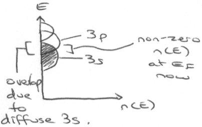
Plots of E(k) –
Semiconductor –
Semiconductors are non-metallic solids, but can still conduct due to the small band gap, which allows thermal excitation of electrons across the band gap and up to the unfilled band.
The Fermi-Dirac Distribution Function governs this:
f(E) = 1/1 + exp[(E-EF)/kT]
This shows a perfect stoichiometry case, with no electrons or holes present in the ground state. At any temperature, the number of holes left in the valence band is equal to the number of excited electrons in the conduction band, and this is what is referred to as an intrinsic semiconductor.
Extrinsic semiconductors require insertion of impurities into the solid to change the properties, a process known as doping.
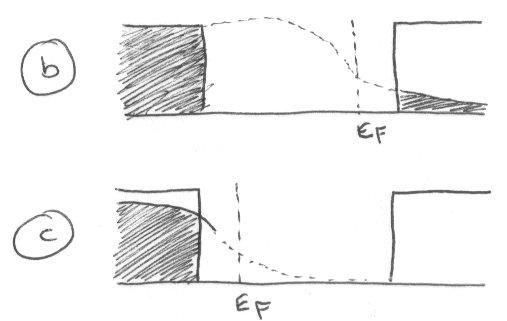
Figure (b) shows an n-type semiconductor. This has more electrons in the conduction band than holes in the valence band. Figure (c) is the p-type with more holes than electrons. Note for both that the Fermi Level is shifted so it is no longer in the middle of the band.
Examples of this is Silicon, which can be doped with Boron so that each Si replaced by B gives rise to 1 missing electron from the valence band (p-type), or conversely doping with Phosphorus leads to more electrons in the conduction band (n-type).
Combining the n and p type semiconductors is the p-n junction, which is a very good conductor, and has many applications, including photovoltaic cells.
The addition of an electron or a hole moves the Fermi Level to just below the conduction band, but the electron is still in the valence band, so thermal excitation is still required. This is because the spare electron is not free, but still localised around the spherical P(+).
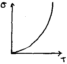
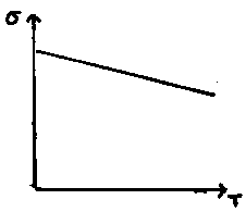
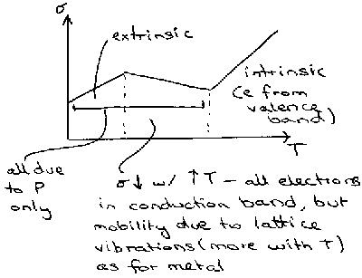
Conductivity in semiconductors is also linked to temperature. The following graph is typical for phosphorus-doped Silicon –
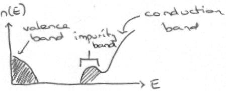
However, as the concentration of impurities is increase, eventually metallic properties are observed. This is due to the formation of an impurity band as impurities’ localisation spheres start to overlap one another amongst the solid lattice. The impurity band typically appears just below the conduction band for the solid, and so tends to behave as a metal assuming there are no electron repulsion factors (see below).
Binding Energies allow the determination of the effectiveness and amount of doping possible. An n-type semiconductor can be modelled as a modified Hydrogenic, which has Energy E = -R/n2.
The modification required is to incorporate the relative permittivity of the solid, εr (a measure of its polarisability) and also use the effective mass, m*. This gives:
E = -R (m*/mo) / n2εr2
This rationalises the energy required to “ionise” a donor electron (i.e. excite into the conduction band).
Also the Bohr Radius for donor states is much bigger than for a hydrogen atom,
an = aHεr / (m*/mo)
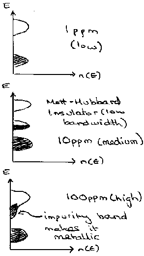
Thus even at low concentration of donor, the wavefunctions of donor states start to overlap. This leads to the metallic behaviour as described above. We can now determine the critical concentration for this behaviour, which is given by the Mott Criterion:
nd1/3an > 0.26
For Phosphorus-doped Silicon, the change in properties follows approximately the following pattern of bands –
Doping in Compound Semiconductors, such as GaAs (III-V) is similar. The n-type is achieved by adding Group IV such as Si to the Ga sites, or alternatively Group VI (Te) to the As. Similarly for p-type, Group II (Be) on Ga or Group IV (Sn) on As. Note that Sn is used for Arsenic, but Si is used for Ga – this reflects the smaller size of Ga(III).
The Hall Coefficient
This is useful for predicting the nature of the conduction in semiconducting materials.

εY is the electric field, jx is the current, and Bz is the magnetic field.
For a free electron, RH = -1/ne (n = number of electrons).
Hole in a nearly filled band: RH = +1/pe (p = hole concentration).
The inverse dependence on concentration implies fewer charges, so each hole / electron must move faster.
Positive RH usually means current is carried more by holes (p-type) than electrons (metal). For example:
NiO – p-type with Ni vacancies.
Ga(III) doped Ge(IV) – p-type.
β-alumina – mobility due to holes left by O (see later).
Chemical Mechanisms for n-type doping in Oxides
- Substitutional displacement of cations in binary compounds by the element to the right in the Periodic Table.
e.g. Sn1-xSbxO2 – very important as becomes metallic at low doping levels and is then an optically transparent metal.
Also Ti1-xVxO2
- Substitutional replacement of O by F or Cl.
e.g. SnO2-xFx
- Interstitial incorporation of donor
NaxWO3 (x > 0.25 is metallic).
HxWO3 (electrochromic).
- Cation excess
Zn1+xO
- Oxygen Deficiency. This is hard to distinguish experimentally from cation excess.
WO3-x, TiO2-x.
- Replacement of countercation exhibiting valency one greater than host ion.
Nd2-xCexCuO4 (n-type oxide superconductor).
Chemical Mechanisms for p-type doping in Oxides
- Substitutional replacement of cation in binary compounds by cation of lower valency.
Ni1-xLixO (some 3d8 oxidised to Ni3+)
- Cation deficiency
La1-xVO3
- Oxygen excess
YBa2Cu3O6.5+x (90K oxide superconductor)
La2CuO4+x
- Replacement of countercation of lower valency.
La2-xSrxCuO4
Semimetal –

An example of this is graphite. Its electronic properties can be greatly influenced by intercalation of anions or cations in between the hexagonal layers of its structure.
Its bands are formed from σ-bonding empty antibonding (like diamond), but 4th valence electron occupies pz → π-bonding.
Intercalating alkali metals or halide ions affects the band structure.
Adding M+ - gives up electrons into π-band (electrons).
Adding X- - remove electrons from lower band (holes).
For example, adding potassium to graphite gives C8K(s), an intercalation compound. K donates an electron to the graphite, so it now conducts far better due to a partially filled antibonding band.
Similarly, Br2 addition to graphite gives C8Br, where Br now accepts an electron from lower graphite bands, which also increases conductivity due to an unfilled lower orbital now.
Note that for the analogous Boron Nitride, the same structure is observed, but the difference in electronegativities between B and N means that the lower band has more N-character, therefore the upper/lower bands don’t touch (its an insulator), i.e. the energy difference in the atomic orbitals is seen in the crystal orbitals. Similarly, intercalation is ineffective in this compound, as M+ can’t populate the higher band (too high in energy), and X- can’t remove electrons from the lower band (more tightly bound).
Effects of electron-electron Repulsions
This is very complicated to model precisely, so approximations are made. One such approximation is the Hubbard Model, which assumes that any important repulsions occur between electrons on the same atom.
In a situation where the overlap between orbitals is very small, 1 electron ends up localised on each atom. This is due to the extra repulsion when trying to move electrons to another atom, i.e.
This is quantified approximately by:
U = I – A
Where I is the ionisation energy of the electron from the metal atom, and A is the electron affinity of putting an electron into an atom that already has one. U constitutes the repulsion energy.
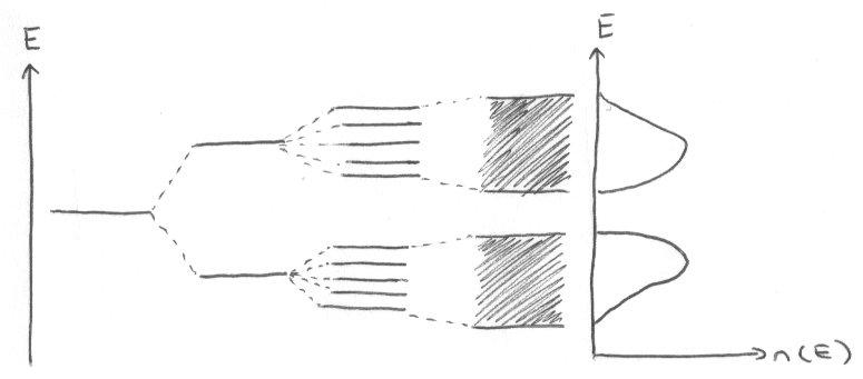
The effect of electron repulsion is to make the half-filled band insulating when interactions between atoms are small.
Increasing band width (W) has an effect on this:
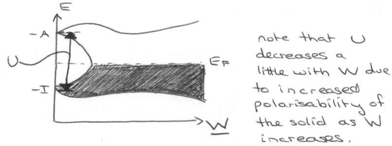
(lower) – I is the Energy of singly-occupied orbitals.
(upper) – A is the Energy of extra electron added to orbitals.
The gap gives the energy required to excite (not the same as the band gap).
These are commonly referred to as sub-bands. The repulsion (U) splitting is the Mott-Hubbard splitting.
Note that the sub-bands broaden by interatomic overlap.
The upshot of this theory is that for metallic conduction, W > U (i.e. no energy gap between sub-bands).
General Trends in Transition Metals
Increasing bandwidth or decreasing electron repulsion leads to delocalised electrons. How can this happen?
1) Position in the Series. Larger d orbitals gives a broader band and smaller electron repulsion. This applies to the early Transition Series or 2nd/3rd row.
This explains the difference between for example NiO and TiO and VO. All these materials have non-zero densities of states at the Fermi level, and so would be expected to be conductors. However, in NiO the interactions with its neighbours are sufficiently weak compared to the internal electron repulsions (W < U) so bands do not form. The reason for this is that Ni is more contracted due increasing nuclear charge with non-compensatory shielding by d electrons, so there is poorer d-d overlap for the less diffuse d orbitals. This is not true for Ti or V which are near the start of the Transition Series, and it is a good conductor. W > U for these metals.
It should be further noted that structure also plays an important part here, as TiO has a structure based on the rock salt structure, but with 1/6th of each element missing in an ordered fashion. This allows contraction and M-M contact (overlap).
2) Oxidation State. This affects metal-metal overlap or indirect covalent bonding via the anion. M-M favoured by low oxidation states, e.g. TiO. Indirect covalency is favoured by high Oxidation States, e.g. ReO3, which is d1 and the 5d orbitals overlap considerably as described for point (1). However, indirect covalent bonding here also favours increased bandwidth, so W > U and it is a good conductor by the Mott-Hubbard Model.
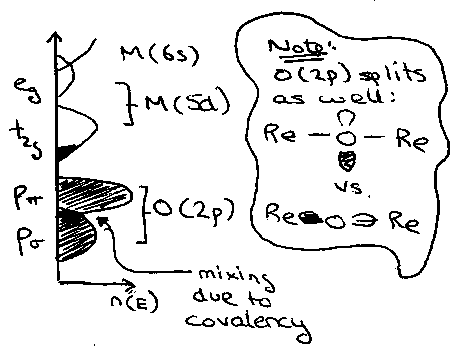
Big orbitals and similar orbital energies from the higher oxidation state mean that conductivity is similar to Copper, even though it is via π-orbitals (Re-O-Re – no direct overlaps). The fact that there is only 1 electron to carry leads to very wide bands.
Note however that this is not the case for WO3, because it possess no d electrons in the +6 oxidation state, so has zero density of states at the Fermi Level.
3) Anion partner. Bandwidth from covalency increase by having a low electronegativity anion, such as the chalcogenides or phosphides. These are typically metallic conductors, while e.g. the halides are not (localised electrons instead).
4) Electron Configuration. Exchange stabilisation of parallel spin electrons contributes to electron repulsion at half-filled shell. For example, MnO is 3d5 and so is less metallic.
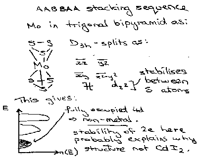
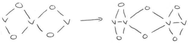
Also, the environment (structure) affects the splitting, so for something that is not Octahedrally coordinated, the electron configuration will change and affect the properties. For example, MoS2 –
5) Other cations, e.g. perovskites (ABO3). The A metal is likely to have empty orbitals a lot higher in energy than the Transition Metal d band. Thus, there is only a small influence. However, for post-transition B metals, s orbitals are now present and may be filled. These have the same energy range as the d orbitals on the Transition Metal. Interaction here leads to band broadening.
For example, consider the transition metal oxides with lithium, Li+[MIIIMIV]O4, which have a spinel-like structure. Electron hopping is likely to be the determining factor here, so looking at the d-electron configurations for the metal will show the likelihood of this:
|
Ti |
d1 |
d0 |
t2g conduction |
|
V |
d2 |
d1 |
t2g conduction |
|
Mn |
d4 |
d3 |
eg conduction |
Often it is the case that Transition Metal solids can undergo changes brought about by temperature or pressure (often instigating a structural change) which affects their electronic properties. It should be noted though that conductivity is not always to do with electron localisation. For example, ligand field splitting will influence conductivity as the d-band is split, as will the filling up of the bands.
WO3 has already been mentioned as having d0 configuration, but this is also true for TiO2. However, this can be doped to be a semiconductor by making O vacancies or adding interstitial atoms. One way of doing this is by adding Lithium metal to form LiTiIIITiIVO4 as described above. Electron hopping is then possible. Note however that adding Na does not have the same effect, because it is less reducing. It will probably aid conductivity a little by doping, but not to the same degree. Also, electron hopping requires a change in structure (bond lengths) in order to transfer the electron (Marcus Theory) so the factors affecting this are important (e.g. eg shifts the bond lengths more, so is less favoured energetically compared to t2g transfer – eg transfer has a higher activation barrier).
In a similar way, WO3 can have Na atoms added to it which enter interstitial sites making a perovskite-like structure. This traps electrons / holes near the band edge and makes an extremely good conductor. NaxWO3 with x = 1 is essentially similar to ReO3 (described above as a good conductor, i.e. W(VI) → W(V) for each Na+) while x < 0.3 is an insulator. This is because with that low a concentration of Na, electrons are trapped around the Na+ (small polaron – Na+ polarises surroundings but the distance between adjacent Na+ is too far – no path for electron).
Its appearance depends on the degree of absorption/reflectance in the visible region (photon energy of 1.5-3eV). This corresponds to the energy gap in the band, since that at a gap of 1.5eV it appears yellow, while at 3eV appears red/purple. The band gap also increases as x increases, so the Na-content can be related to the solids’ colour.
Many Transition Metal Oxides show semiconducting properties. Two such examples are ZnO and NiO. Mott-Hubbard Theory explains why they are not conductors, that is that electrons do not move between because of e-e repulsions – localised electrons as opposed to a band. Ni and Zn interact weakly with neighbours due to contracted d orbitals that do not overlap well, so the bands narrow. The band gap is in fact rather large, but non-stoichiometry leads to the semiconductivity (they would be insulators).
NiO is a p-type semiconductor – it has Ni vacancies (holes). Increasing the pressure of O2 oxidises the NiO, which generates more Ni vacancies and thus increases conductivity. Ni3+2xNi2+1-3xO forms which is O-rich (x Ni vacancies with x additional O). A similar effect is observed when adding Li2O to the NiO, as Li+ entering causes Ni2+ to form Ni3+ and also generates holes (in the t2g band). This is extrinsic doping and aids conductivity. Ni3+ is d7, and has a vacancy in the eg which allows transfer of an electron without pairing up electrons, so it hence conducts far better (x109). The only problem is that Ni-O bond lengths differ for the two oxidation states, which gives a higher activation energy.
ZnO is an n-type semiconductor due to interstitial Zn. This means an excess of electrons are present. Increasing the pressure of O2 leads to oxidation of the ZnO. This has the effect of removing the electrons, making it less conducting.
Metal-Insulator Transitions
These have a large effect on conductivity, for example:
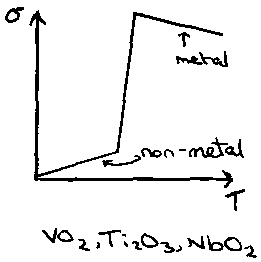
Non-metal – Metal Transition, e.g. VO2, Ti2O3, NbO2:
Non-metal – Non-metal Transition, e.g. Fe3O4:
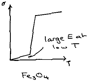
These are typically due to structural changes occurring (often as a result of a temperature change). For example, consider Fe3O4, a mixed valence compound. The Hubbard Model assumes half-filled bands, although any integral number of electrons is possible. Adding extra electrons allows for them to move from atom to atom without extra repulsion. This is known as electron hopping.
This would lead to the prediction that mixed valency of non-stoichiometric solids should be metallic regardless of electron repulsion factors (U) or band width (W). This is not true, and can be explained by considering the narrow bands that form, so that lattice distortions trap the extra electrons or holes that have formed to allow for conduction, so that it cannot occur. An exception is Fe3O4. This shows high conductivity at normal Temperature, and is a consequence of the electron hopping phenomenon, via an Fe2+ ↔ Fe3+ transfer. This is possible because this has the inverse spinel structure, so both Fe2+ and Fe3+ sit in octahedral holes which allows the transfer. However, cooling to below 135K stops the process and it behaves as a semiconductor.
Another example of a structural change that facilitates electron transfer is found for Ti2O3, which goes from semiconductor to metallic conductor at ~200oC. There is variable stoichiometry, and also a structural change that occurs.
VO2 is another example of a metal-insulator transition. It is best explained by considering Peierls Distortion.
Peierls Distortion
This occurs in 1 dimensional chains, due to a metallic state being unstable with respect to a lower energy state with zero density of states at the Fermi level.
For example, polyacetylene can be viewed as a series of alternating single and double carbon bonds in a chain, with p orbitals perpendicular to the chain allowed electrons to be transferred along it. There is 1 electron in each of these orbitals, so it is half-filled and has a non-zero n(E), so we would expect it to be metallic. It isn’t, but instead semiconducts.
The reason for this is that a structural distortion occurs which lowers the energy, and a band gap opens up at the Fermi level as a consequence. This can be seen as comparable to Jahn-Teller distortion in certain octahedral complexes to lower their energy.
Thus, a split occurs from:
Thus, bond alternation along the chain is in fact seen, and it is not fully delocalised as we might expect. The process is electronically driven.
The effect is also seen for VO2, which has the rutile structure made up of VO6 octahedra edge sharing. This leads to strong overlapping d orbitals in 1 dimension, and V4+ is d1 so half-filled. At high temperature, VO2 is metallic as we might expect, but < 68oC it becomes an insulator due to structural (Peierls) distortion.
Alternating long and short bonds are seen as for polyacetylene, and this allows for V-V contacts which localise the electrons in the V-V bonds.
Peierls Distortion is suppressed by:
- Increase in dimensionality, e.g. polyacene undergoes 2D Peierls Distortion, but it has much less effect.
- Pressure broads the bands and so removes the driving force to obtain lower Energy.
- Filling of the bands, e.g. with S,Se,Te anions.
NbO2 also shows a similar distortion, and is non-metallic except at high temperatures, where metal-metal bonding is stronger. It has 4d1 electron configuration. MoO2 and WO2 (d2) also distort in a similar way, but they are still metallic despite this due to that extra electron. RuO2 would also expect to be distorted (4d4) but in fact adopts a different (rutile) structure to avoid the Ru-Ru antibonding occupation if it did distort.
Platinum Chain Compounds
These were the first one dimensional conductors found. They are based on K2Pt(CN)4.3H2O. This is in fact an insulator but when dissolved in water and oxidised with a little bromine, copper coloured needles of [K2Pt(CN)4]Br0.3.3H2O crystallise out. This is commonly known as KCP. The KCP crystals contain chains of close packed square planar Pt(CN)42- units, and the conductivity parallel to the chains is 104 times that perpendicular. This is because the ligands ensure inter-chain separation is large, so there is no overlap of Pt orbitals. The bromide ions are arranged randomly in the centre of the effective unit cell. The 5d orbital on the Pt atoms in a chain overlap well using the dz2 orbitals as a basis. In the parent compound there are just enough electrons to fill the band that results due to this overlap, so the compound is an insulator. Bromine takes up electrons from this band to form bromide ions, resulting in a partially filled band and metallic conductivity.
An unusual property is its temperature dependence. Below 150K the conductivity drops sharply, contrary to that expected of metals. This is due to Peierls distortion as this is a one dimensional conductor, as discussed above.
Many Pt chain compounds have been made based on KCP. This usually involves using chloride or bifluoride in place of bromide, and sometimes cation deficient variations. Note that the ligands attached to Pt must always be sufficiently small to allow chains to form.
Other One Dimensional Solids.
One particular example is chains composed of stacks of 2 unsaturated cyclic molecules arranged alternately. The first one discovered was TTF-TCNQ. The electrical conductivity of this is good at room temperature and increases with decreasing temperature until about 80K. The conductivity drops in the same way as KCP. TCNQ is a good electron acceptor, and in TTF-TCNQ the columns of each type of molecule interact to form delocalised orbitals. Some electrons from the highest energy filled band of TTF move across to partly fill a back of TCNQ, so that both types of columns have partially occupied bands. This partial transfer only occurs with molecules whose electron donor ability is neither too small nor too large (e.g. TTF). This is because very good electron donors such as alkali metals transfer one electron per TCNQ, and the acceptor band becomes full. In TTF-TCNQ this corresponds to about 0.69 electrons per molecule. These types of conductors are often referred to as molecular metals.
Superconductors –
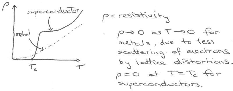
These can be identified by the Meissner Effect – superconductivity leads to expulsion of lines of magnetic flux that run through a sample (perfect diamagnetism).
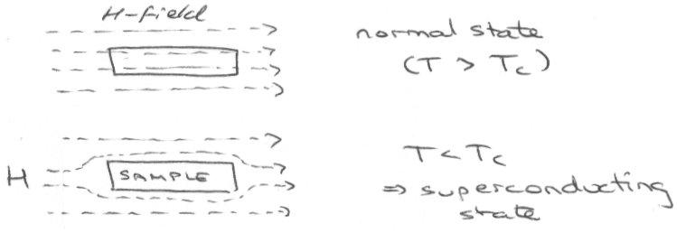
Flux can eventually enter for some superconductors, particularly Cuprates, and it then ceases to superconduct.
Theories to explain the phenomenon are mathematically complex, and although superconduction in elements and alloys has been satisfactorily explained, there is still no strong theory on why the effect occurs at the much higher temperature for perovskite based cuprates.
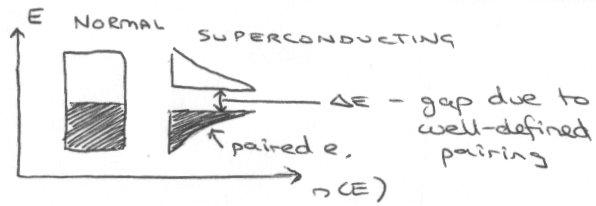
Bardeen Cooper Schrieffer Model
In the BCS Model, charge is carried by 2 electrons coupled together (Cooper pairs) not 1 electron. This is surprising since 2 x electrons normally repel!
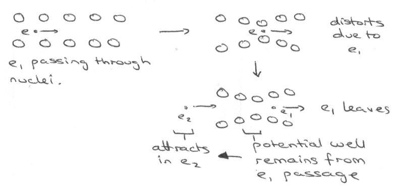
The Cooper pair has zero spin so obeys Bose-Einstein statistics (it’s a Boson), so it can enter the same quantum state so the “gas” of paired electrons in the superconducting state is a macroscopic quantum object. Below Tc, thermal energy is insufficient to overcome the attractive interaction, so current carriers are not scattered by thermal vibrations (zero DC resistivity).
The diagram above comes about from interactions between lattice and electron vibrations. This would predict an isotope effect on interchange, and also that Tc increases as the number of electrons close to the Fermi energy increases. Both these are shown well by superconducting K3C60. The BCS Model also works for “standard” superconductors such as Nb3Ge and MgB2.
Perovskite-based High Temperature Superconductors
e.g. YBa2Cu3Ox , La2-xBa2CuO4.
As mentioned, it is not followed by the cuprates. For these, charge carriers are zero-spin electron pairs, but there is no isotope effect so the mechanism does not involve lattice vibrations. This is still being researched.
Also, BCS Model predicts a maximum Tc of ~40K, whereas these “high” temperature superconductors have been made to superconduct at ~ 150K (HgBa2Ca2Cu3O8+δ).
They can be considered as modified Ln2CuO4 (which is a Mott-Hubbard insulator), and then doping splits into bands of CuI/CuII and CuII/CuIII (filled) via oxidation and reduction by the doping agent. This gives holes and electrons respectively, and promotes electron hopping.
The Cooper pair formation is thought to be due to extremely strong superexchange interactions between Cu spins (not electron vibrations as this would give rise to lattice distortions).
Zeolites – see advanced notes.
B) Defects and Ionic Conductivity
Point Defects
These are single lattice site perturbations. The simplest types are lattice vacancies or interstitial atoms added. However, this often leads to a build up of charge in the crystal, and this gives a very high electrostatic potential, so only a few can ever be tolerated.
Far more common are defects that compensate for this charge build up.
Schottky defects are one such defect. This is where there is both an anion and cation vacancy as a pair. This allows the charge to balance.
Schottky Defect:
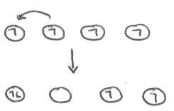
Similarly, Frenkel defects involve balancing a vacancy by an interstitial atom of the same type. In this case it can be confined to one kind of ion, e.g. in silver halides, often the Ag+ shows Frenkel defects, but there are few defects amongst the X-.
Frenkel Defect:
Other defects have already been mentioned, such as creating holes or adding electrons to solids to compensate for charge – this leads to interesting electronic properties such as enhanced semiconductivity. These are more common amongst the Transition Metals because of their ability to vary Oxidation State to accommodate this (e.g. the electron can enter into the d band).
Thermodynamically, the energy to form a defect pair can be written as U = nw, which ultimately rearranges to:
n/N = e-w/2kT
(when n is assumed small)
This represents a balance between the energy loss in forming a defect and the entropy gained in doing so.
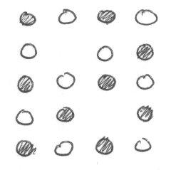
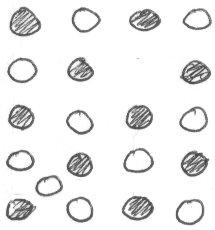
There are also a number of non-stoichiometric defects, the most common of which are Colour Centres, particularly seen in alkali halides.
F-centre – where an anion vacancy has trapped one electron.
F’-centre – 2 electron excess.
FA-centre – F-centre with adjacent cation impurity.
F2-centre – 2 adjacent F-centres.
VK-centre – trapped hole due to an X2- molecular ion formation.
H-centre – neutral anion interstitial (X2- formation again, but now adjacent).
Non-stoichiometry is also seen in e.g. Fe1-xO and TiO2-x. Stabilisation is provided by entropy factors.
There are also extended defects, which are typically linear or planar. The main type of linear defect is dislocation, where the arrangement of a line in the crystal lattice has been changed.
There are many planar defects. Shear planes (such as in WO3-x) are where O vacancies have congregated into a plan, which brings Metal atoms closer together. Grain Boundaries often form between 2 crystallites in ceramics.
Another planar defect is the crystal surface itself, which is rarely smooth which indicates many types of defects occurring to give the rough texture.
Ionic Conductivity and Solid Electrolytes
It is possible for ionic structures to conduct electricity not just when molten or dissolved into ions, as long as there is the possibility of movement of the ions in the structure so that the electrons can be transferred. Unsurprisingly, this is usually possible as a result of either structural changes or defects in the crystal structure.
For example, NaCl often has Schottky Defects like so:
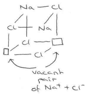
Cl- and Na+ vacant pairs allows for ion mobility. Doping with CaCl2 further enhances this as each Ca2+ occupies 2 x Na+ and creates a cation vacancy (extrinsic doping).
Adding more Na to NaCl forms a compound of the form Na1-xClex with many F-centres forming. Anion vacancy traps the electrons as described and this compensates the charge of the missing anion. This conducts very well under irradiation, i.e. photoconduction, as the electron can be promoted into the conduction band.
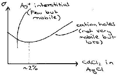
AgCl is similar, but shows Frenkel defects:
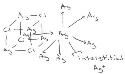
Addition of Cd2+ to this actually decreases the conductivity, because the vacancies due to its +2 charge balancing limit the interstitial Ag+ concentration which allows for conduction. However, when Cd2+ concentration becomes high enough, the trend seen for Ca2+ in NaCl takes over, and conductivity increases as a result of many vacancies now present. This can be shown in the following graph:
Fast-ion Conductors exist that have conductivity approaching that of molten salts or electrolyte solutions. Some examples follow.
Zirconia, ZrO2, has the cubic fluorite structure at high temperature (it is 7 coordinate at room temperature). This can be stabilised at room temperature by adding CaO. Ca2+ occupies the Zr4+ site, so O2- vacancies develop. There is a high proportion of CaO present to stabilise this form, which means lots of vacancies form. This leads to O2- anion conduction using these vacancies to move, and it is very rapid.
Doping can also be carried out by using M2O3 (M = Yttrium or lanthanides) which has the same effect. Similar conductivity is also seen for CeO2, where the cubic fluorite structure is again stabilised in much the same way.
Typical molecular formulas are:
Zr1-xYxO(2-x)/2[]x/2
Ce1-xYxO(2-x)/2[]x/2
Zr1-xCaxO(2-x)[]x ( 0 < x < 0.15 ideal)
High concentrations of doping actually causes a drop in conductivity however. This is because the vacancies that it creates begin to order themselves. Similar trends then to the AgCl + CdCl2 – conductivity governed by Frenkel vs. holes.
Bi2O3 has a low symmetry monoclinic structure at low temperature. Above 730oC it forms cubic fluorite but with ¼ cation sites vacant, giving BiO1.5[]0.5. This is an excellent O ion conductor above this temperature.
High temperature phase is stabilised by Y2O3, or similar. This retains good ionic conductivity down to lower temperatures, while being less good at high temperature.
These properties are probably due to the high polarisability of Bismuth.
Na-β-alumina has the formula Na2O . 11 Al2O3 although the stoichiometry varies and there are a range of compounds of M2O . nX2O3 where n = 5-11, with M having +1 charge, and X having +3 charge.
The fast conduction comes about from the crystal structure adopted. It forms close-packed layers of oxide, but every fifth layer has ¾ of the O missing. Al3+ fits into the Octahedral and Tetrahedral holes, then strong Al-O-Al bridges form every 5 layers. Na+ sits in this bridging layer, and is highly mobile due to the many vacancies left by O, and that Na+ is in fact smaller than O2-. Thus, conduction occurs within these conduction planes containing O2- vacancies.
Increasing n (8-11) leads to a slightly different structure (β’’-alumina) which has even higher conductivity, but tends to be sensitive to moisture.
Silver Iodide is another compound that is a fast ion conductor. This only occurs for the α-AgI phase, which forms at > 146oC. This is again due to structure, as this phase constitutes a BCC lattice of I-, and the central I- thus has roughly 14 nearest neighbours in an (irregular) rhombic dodecahedron. This allows many positions for the Ag+ to occupy, actually: 6 x distorted Octahedral, 12 x Tetrahedral, 24 x Trigonal, for only 2 Ag atoms! It has since been shown that it only uses the tetrahedral sites, but still can move between these via the trigonal sites easily, since Coordination Number 4→3→4 is facile (very low Activation Energy). In this way, it can be regarded as a molten sub-lattice.
The features that contributed to this in AgI were:
- Charge on ions is low,
- Coordination number is low (low Activation Energy),
- Polarisable anion (eases passage of cation since X- is deformable),
- Lots of vacancies.
Lithium Ion Batteries
Electrochemical implications – making a more powerful and rechargeable battery. Works by using intercalation then deintercalation into oxides.
Consider ternary LiCoO2, which is in fact layered (not common for TM oxides) due to ordering between Li+ and Co3+. It is oxidised electrochemically to Li0.5CoIII/IVO2 with deintercalation of lithium metal, but preservation of the structure. The reverse reductive intercalation reaction to restore the composition is favourable and has a constant thermodynamic driving force of +4.0V. This is the basis of the Li-ion battery, since it is rechargeable and it also has the benefit of a large power/mass ratio (good in e.g. mobile phones). Deintercalation = charging, intercalation = discharge during use.
Other metals have been substituted in to try to develop batteries that last longer and are more powerful. Using TiIII/TiIV proved to be insufficiently powerful (2.5V) even though it is fully reversible, which would have great consequences for capacity. MnIII/IV was also tried out, and its power rating is 3.5V and gives the entire range of reversibility as well (unlike Co). It is also cheaper and less toxic. The problem however is that MnIII is d4 and therefore undergoes Jahn-Teller distortion which hampers reversibility as the electrode structure breaks down after many cycles.
Experimental Methods
There are a variety of techniques available for probing the structures of solids. In terms of looking at their electronic properties, the typical ones are:
Optical Absorption Spectroscopy –
Band gaps may be probed by absorption, but above the band gap, info is convoluted about filled and empty densities of states. Also, there are problems in highly ionic solids because the absorption threshold may be associated with excitons. This means that an excited electron remains trapped by the Coulombic Potential associated with hole in the valence band, and causes an extra peak to appear prior to the conduction band, stopping the true value of the band gap being determined.
Also, you cannot assume that the amount of radiation absorbed is simply related to the amount transmitted, because this ignores reflection.
Metals have zero band gap, but absorption spectroscopy struggles to show this because below a critical energy (the plasma energy) metals have very high reflectivity. Ep is related to concentration of conduction electrons (n). Typically, the plasmon energy (h(bar)ωρ) is in the UV range, so reflects in the visible and has a shiny appearance.
For example, NaxWO3 (0 < x < 1) can be thought of as diluted Na with much lower n. Ep is in the visible range and varies with x:
Low x → red end of spectrum → blue appearance
Medium x → purple appearance
High x → blue end of spectrum → golden yellow appearance.
Photoelectron Spectroscopy – this is particularly useful as it can fully probe the bands fully (subject to limitations of Koopmans’ Theorem) by varying the photoelectron energy, so that band intensities vary.
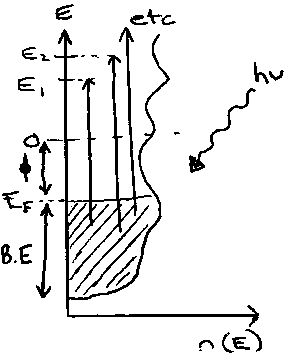
KE = hν – BE – φ
Kinetic energy = photon energy – binding energy (rel. to EF) – workfunction
e.g.
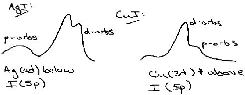
Also shows where d-orbitals lie by cross-section effects (the probability that a photon of a given energy will ionise an orbital of a given type).
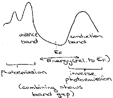
Inverse PES gives good information on occupied orbitals (by ionising those electrons) and reversing the technique allows information about the empty bands to be determined.
It works on the “electron in, photon out” approach (i.e. the opposite of PES). Incoming electrons always decay with loss of energy and ends up in an empty state of the solid. Photons are emitted and counted by a detector which only accepts photons of a single fixed energy.
Example of full PES analysis: SiO2 –
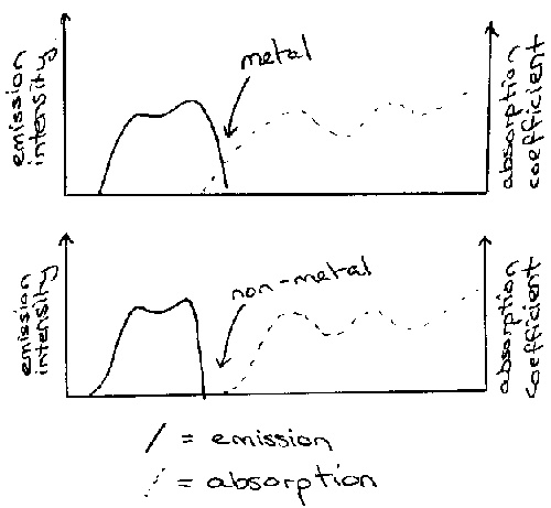
X-ray Emission and Absorption
X-ray Emission probes the filled levels, while X-ray Absorption is harder to do and more expensive, but gives information about empty levels.
Combining the techniques gives the band structure. It involves the core level which exhibits no band structure broadening effects (subject to lifetime broadening) – direct probe of filled and empty density of states results.
Electron Energy Loss – gives information about conducting electrons.
- –
I am happy for them to be reproduced, but please include credit to this website if you're putting them somewhere public please!